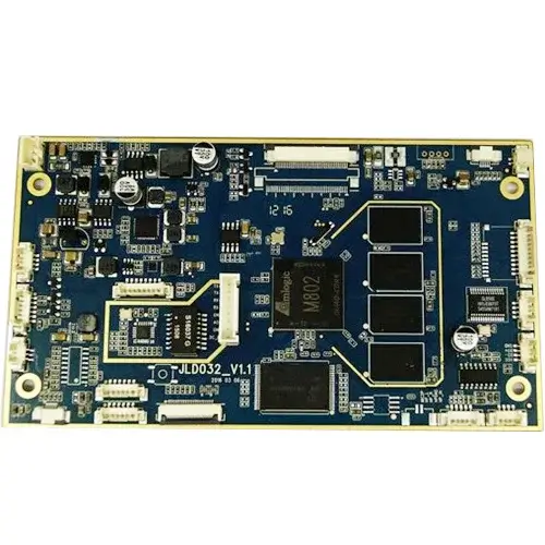
Miniaturization & High Density
Uses HDI (High-Density Interconnect) and multilayer PCBs to fit complex circuits into small form factors (e.g., smartphones, TWS earbuds).
Microvias (laser-drilled) and fine-pitch components (0201, 01005 sizes) for space-saving designs.
High-Speed Signal Integrity
Optimized for high-frequency signals (5G, Wi-Fi 6, Bluetooth).
Controlled impedance routing and EMI shielding to prevent interference.
Cost-Effective Mass Production
Uses surface-mount technology (SMT) for automated, high-volume assembly.
Balances performance with DFM (Design for Manufacturing) to reduce costs.
Flexible & Wearable PCBAs
Flex PCBs and rigid-flex PCBs for bendable devices (smartwatches, foldable phones).