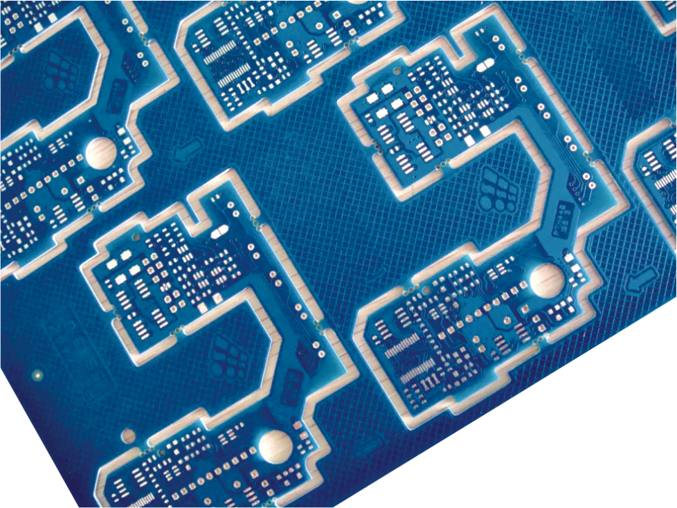
Advantages:
Miniaturization: Ideal for slim devices (smartphones, wearables, IoT).
Enhanced Performance: Reduced signal loss and improved EMI shielding.
Reliability: Dense interconnections reduce failure points.
Applications:
Consumer electronics (5G phones, tablets), automotive ADAS, medical devices, aerospace systems.